← Cara Merakit Driver Micro M2 Bostrab: Panduan Lengkap untuk Pemula! Cara humana: anatomía, estructura y función 2SA1216/2SC2922: Store Home Products and Feedback Guide! Transistor sanken 5dy 2sa1216 2sc2922 / a1216 c2922 rrt →
If you are looking for Mixed signal PCB layout help - Page 1 you've visit to the right page. We have 25 Pictures about Mixed signal PCB layout help - Page 1 like Basic Guidelines for Mixed-Signal PCB Layout Design _ Electronic Design, Basic Guidelines for Mixed-Signal PCB Layout Design - Utmel and also Overlapping Planes in PCB Mixed-Signal Layouts | Blog | Altium Designer. Here it is:
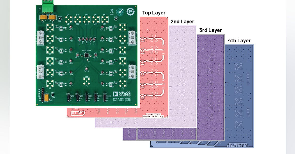
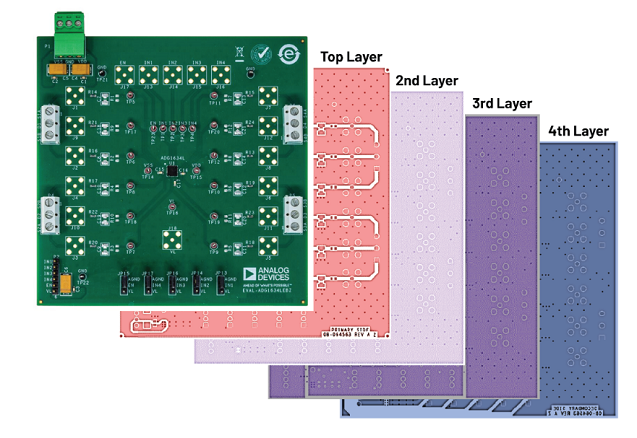
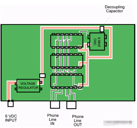
Mixed Signal PCB Layout Help - Page 1
Mixed signal PCB layout help - Page 1
Basic Guidelines For Mixed-Signal PCB Layout Design | Electronic Design
 www.electronicdesign.com
Basic Guidelines for Mixed-Signal PCB Layout Design | Electronic Design
Overlapping Planes In PCB Mixed-Signal Layouts | Blog | Altium Designer
 resources.altium.com
Overlapping Planes in PCB Mixed-Signal Layouts | Blog | Altium Designer
Overlapping Planes In PCB Mixed-Signal Layouts | Blog | Altium Designer
 resources.altium.com
Overlapping Planes in PCB Mixed-Signal Layouts | Blog | Altium Designer
Mixed Signal PCB Layout
 www.linkedin.com
Mixed Signal PCB Layout
Mixed-Signal Hardware/PCB Design Tips - Phil's Lab #88
 home.fedevel.com
Mixed-Signal Hardware/PCB Design Tips - Phil's Lab #88
Basic Guidelines For Mixed-Signal PCB Layout Design - Utmel
 www.utmel.com
Basic Guidelines for Mixed-Signal PCB Layout Design - Utmel
Basic Guidelines For Mixed-Signal PCB Layout Design - Utmel
 www.utmel.com
Basic Guidelines for Mixed-Signal PCB Layout Design - Utmel
Basic Guidelines For Mixed-Signal PCB Layout Design (Download
 www.electronicdesign.com
Basic Guidelines for Mixed-Signal PCB Layout Design (Download ...
Basic Guidelines For Mixed-Signal PCB Layout Design - Utmel
 www.utmel.com
Basic Guidelines for Mixed-Signal PCB Layout Design - Utmel
What Is A Mixed-signal PCB And How To Design It?
 pcbassemblymanufacturing.com
What is a mixed-signal PCB and how to design it?
Basic Guidelines For Mixed-Signal PCB Layout Design - Andwin Circuits
 www.andwinpcb.com
Basic Guidelines for Mixed-Signal PCB Layout Design - Andwin Circuits
Basic Guidelines For Mixed-Signal PCB Layout Design - Andwin Circuits
 www.andwinpcb.com
Basic Guidelines for Mixed-Signal PCB Layout Design - Andwin Circuits
Adc - Mixed Signal PCB Layout For PSoC - Electrical Engineering Stack
 electronics.stackexchange.com
adc - Mixed signal PCB layout for PSoC - Electrical Engineering Stack ...
Basic Guidelines For Mixed-Signal PCB Layout Design | Electronic Design
 www.electronicdesign.com
Basic Guidelines for Mixed-Signal PCB Layout Design | Electronic Design
Mixed Signal Pcb Layout Guidelines - Design Talk
 design.udlvirtual.edu.pe
Mixed Signal Pcb Layout Guidelines - Design Talk
Basic Guidelines For Mixed-Signal PCB Layout Design - Utmel
 www.utmel.com
Basic Guidelines for Mixed-Signal PCB Layout Design - Utmel
Basic Guidelines For Mixed-Signal PCB Layout Design _ Electronic Design
 www.scribd.com
Basic Guidelines for Mixed-Signal PCB Layout Design _ Electronic Design ...
Basic Guidelines For Mixed-Signal PCB Layout Design - PCB Manufacturing
 www.andwinpcb.com
Basic Guidelines for Mixed-Signal PCB Layout Design - PCB manufacturing ...
Basic Guidelines For Mixed-Signal PCB Layout Design - Utmel
 www.utmel.com
Basic Guidelines for Mixed-Signal PCB Layout Design - Utmel
Mixed Signal PCB Layout Help - Page 1
Mixed signal PCB layout help - Page 1
Adc - Mixed Signal PCB Layout For PSoC - Electrical Engineering Stack
 electronics.stackexchange.com
adc - Mixed signal PCB layout for PSoC - Electrical Engineering Stack ...
Mixed Signal PCB Layout Help - Page 1
Mixed signal PCB layout help - Page 1
What Is A Mixed-signal PCB And How To Design It?
 pcbassemblymanufacturing.com
What is a mixed-signal PCB and how to design it?
Mixed Signal PCB Layout Help - Page 1
Mixed signal PCB layout help - Page 1
What is a mixed-signal pcb and how to design it?. Basic guidelines for mixed-signal pcb layout design _ electronic design .... Basic guidelines for mixed-signal pcb layout design