← Design Your Own Arduino Uno Board with Eagle – Step-by-Step Guide! design principles: understanding the fundamentals Class GB Power Supply: The Ultimate Guide to Building Your Own Audio Gear! Noon weather thursday 6/26/2025 →
If you are searching about Pcb Layout Drawing you've visit to the right place. We have 25 Pictures about Pcb Layout Drawing like A detailed guide to PCB layout design - IBE Electronics, Best Practices For Designing A Pcb Layout Circuit Bas - vrogue.co and also Pcb designing, pcb layout, simulation on proteus, simulink by. Read more:
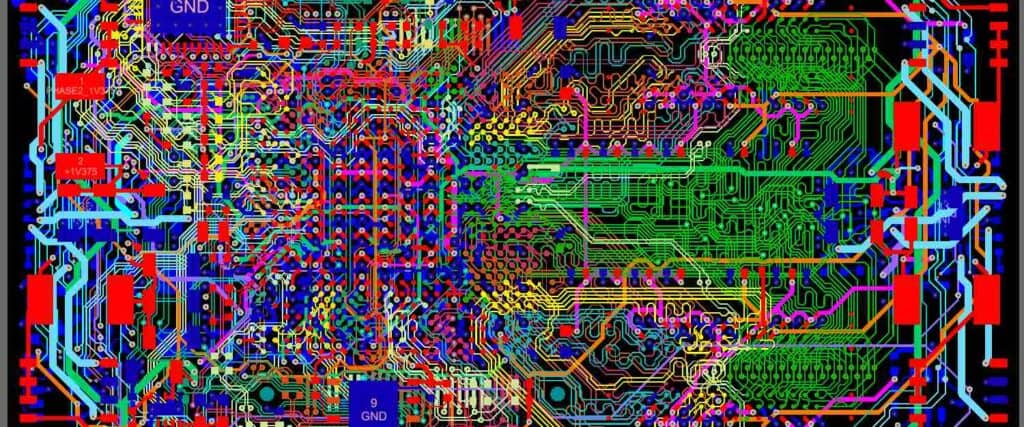
Pcb Layout Drawing
 mavink.com
Pcb Layout Drawing
Pcb Designing, Pcb Layout, Simulation On Proteus, Simulink By
 www.fiverr.com
Pcb designing, pcb layout, simulation on proteus, simulink by ...
Workshop On PCB Designing 2023, Top Engineers, Workshop, Chennai
 www.knowafest.com
Workshop on PCB Designing 2023, Top Engineers, Workshop, Chennai
Reparator Credential Dumnezeu Pcb Design Guidelines Releu Alb Ca
 cristor.dz
Reparator Credential Dumnezeu pcb design guidelines releu alb ca ...
Pcb Manufacturing Process Step By Step Tutorial With Flow Chart
 www.sexiezpix.com
Pcb Manufacturing Process Step By Step Tutorial With Flow Chart ...
Pcb Designing, Pcb Layout, Simulation On Proteus, Simulink By
 www.fiverr.com
Pcb designing, pcb layout, simulation on proteus, simulink by ...
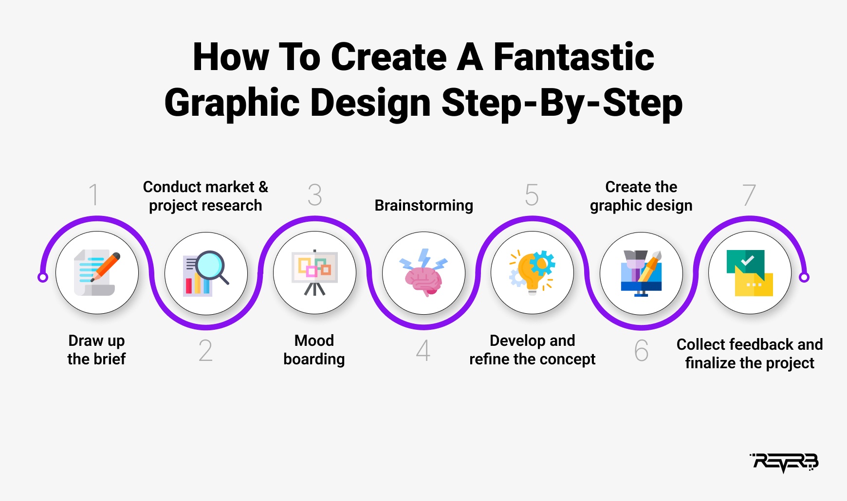
A Step By Step Guide To The Logo Designing Process - Vrogue.co
 www.vrogue.co
A Step By Step Guide To The Logo Designing Process - vrogue.co
ChatGPT Tutorial: A Step-by-step Guide For Beginners
 mindtastik.com
ChatGPT Tutorial: A step-by-step guide for beginners
Convert Schematic To Pcb Layout Using Proteus
 www.circuitdiagram.co
Convert Schematic To Pcb Layout Using Proteus
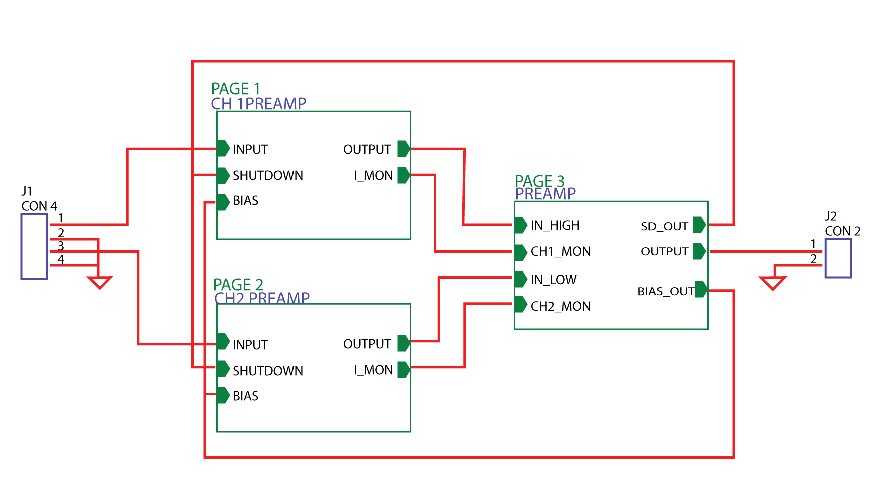
Schematic Diagram Pcb Layout
 wiringfixryan.z21.web.core.windows.net
Schematic Diagram Pcb Layout
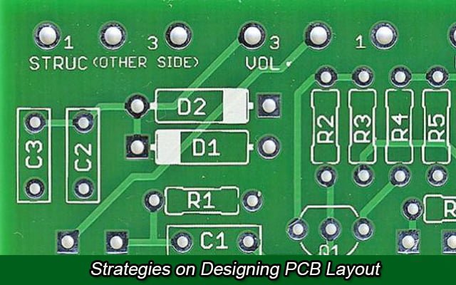
Complex PCB Design: Tips And Best Practices For Successful
 hillmancurtis.com
Complex PCB Design: Tips and Best Practices for Successful ...
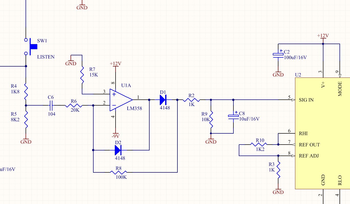
Pcb Schematic And Layout
 manualdataoddfellows.z21.web.core.windows.net
Pcb Schematic And Layout
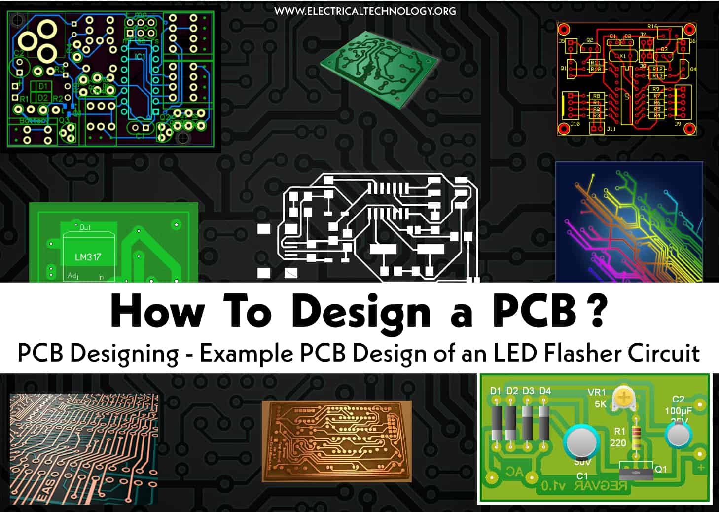
PCB Designing: How To Design A PCB - Step By Step Guide
 hasnafriedchicken.com
PCB Designing: How To Design a PCB - Step by Step Guide
PCB Layout Checklist - Finish Line Product Development
 finishlinepds.com
PCB Layout Checklist - Finish Line Product Development
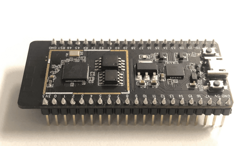
Features And Specifications Of ESP32 PCB – Hillman Curtis: Printed
 hillmancurtis.com
Features and Specifications of ESP32 PCB – Hillman Curtis: Printed ...
Best Practices For Designing A Pcb Layout Circuit Bas - Vrogue.co
 www.vrogue.co
Best Practices For Designing A Pcb Layout Circuit Bas - vrogue.co
A Detailed Guide To PCB Layout Design - IBE Electronics
 www.pcbaaa.com
A detailed guide to PCB layout design - IBE Electronics
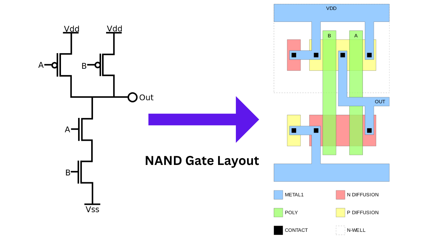
Nand Gate Cmos Diptrace Pcb Layout
 mavink.com
Nand Gate Cmos Diptrace Pcb Layout
Reasonable Price And High Quality For PCB Schematics Designing, PCB
 aac3dc2e8ac4a117.en.made-in-china.com
Reasonable Price and High Quality for PCB Schematics Designing, PCB ...
High Speed Pcb Layout Guidelines - Design Talk
 design.udlvirtual.edu.pe
High Speed Pcb Layout Guidelines - Design Talk
High Quality Designing Pcb Layout And Electronics Devices Manufacturing
 www.alibaba.com
High Quality Designing Pcb Layout And Electronics Devices Manufacturing ...
10 Step-by-Step "How-to" Guide Templates - Venngage
 venngage.com
10 Step-by-Step "How-to" Guide Templates - Venngage
Pcb Design Flow Steps For Designing Pcbs For Manufacturing – Eroppa
 eroppa.com
Pcb Design Flow Steps For Designing Pcbs For Manufacturing – eroppa
Wall Framing Layout Step By Step: A Comprehensive Guide To Perfect Wall
 www.coohom.com
Wall framing layout step by step: A Comprehensive Guide to Perfect Wall ...
PCB Creepage And Clearance Criteria In Designing PCB Layout - Kingford
 www.kingfordpcb.com
PCB Creepage and Clearance Criteria in Designing PCB Layout - Kingford
High quality designing pcb layout and electronics devices manufacturing. pcb schematic and layout. Features and specifications of esp32 pcb – hillman curtis: printed ...