← Introduction to PCB Design: Complete Guide to Aging Test Methods! Thermal aging: how to test pcba against heat and humidity Desain Papan Sirkuit Cetak (PCB) – Everything You Need to Know! Ic pada pcb papan sirkuit cetak dengan perangkat yang dipasang di ... →
If you are searching about PCB footprint land pattern design. a Layout design for the MMIC LNA b you've visit to the right web. We have 25 Images about PCB footprint land pattern design. a Layout design for the MMIC LNA b like 2 Front To Back MMIC Design Flow With ADS | PDF | Simulation, [REDIRECT] Virtuoso RF Solution | Cadence and also MMIC phase shifter 45 degree bit design. Here you go:
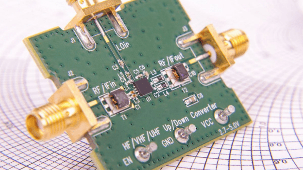
PCB Footprint Land Pattern Design. A Layout Design For The MMIC LNA B
 www.researchgate.net
PCB footprint land pattern design. a Layout design for the MMIC LNA b ...
A Guide To The RF PCB Design
 hillmancurtis.com
A Guide to the RF PCB Design
MMIC Phase Shifter 45 Degree Bit Design
 www.microwaves101.com
MMIC phase shifter 45 degree bit design
Rf Pcb Layout
 mavink.com
Rf Pcb Layout
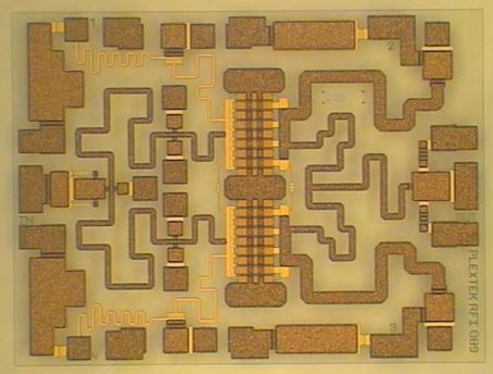
Layout Design Of Elliptic Multilayer CPW MMIC LPF | Download Scientific
 www.researchgate.net
Layout Design of elliptic multilayer CPW MMIC LPF | Download Scientific ...
[REDIRECT] Virtuoso RF Solution | Cadence
![[REDIRECT] Virtuoso RF Solution | Cadence](https://www.cadence.com/content/dam/cadence-www/global/en_US/images/Products/mmic-awr.jpg) www.cadence.com
www.cadence.com
[REDIRECT] Virtuoso RF Solution | Cadence
2 Front To Back MMIC Design Flow With ADS | PDF | Simulation
 www.scribd.com
2 Front To Back MMIC Design Flow With ADS | PDF | Simulation ...
3 Enhanced Basics Of RF/Microwave PCB Design | MV Flex Circuit
 www.flexiblepcbboard.com
3 Enhanced Basics of RF/Microwave PCB Design | MV Flex Circuit
Layout Of The Two-stage Broadband MMIC PA. | Download Scientific Diagram
 www.researchgate.net
Layout of the two-stage broadband MMIC PA. | Download Scientific Diagram
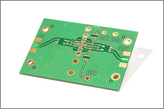
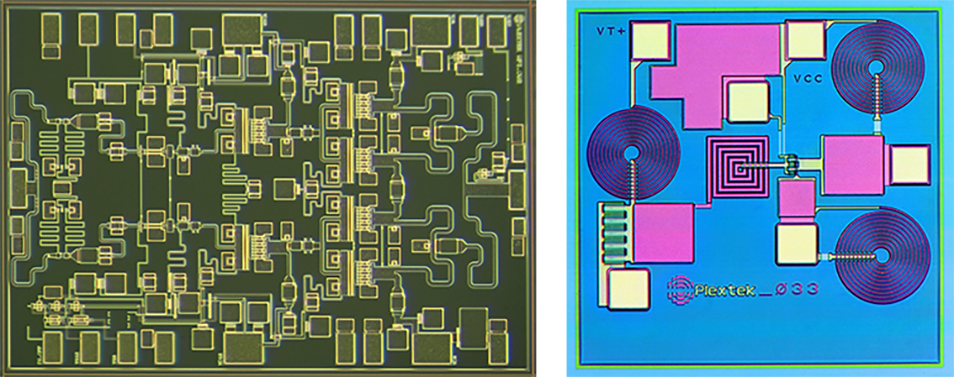
Details Of The Circuit Board Layout Design For The MMIC Low Noise
 www.researchgate.net
Details of the circuit board layout design for the MMIC low noise ...
Design Services: GaN MMIC | CML Micro Design Services: MMIC, RFIC
 www.prfi.com
Design Services: GaN MMIC | CML Micro Design Services: MMIC, RFIC ...
MMIC Phase Shifter 90 Degree Bit Design
 www.microwaves101.com
MMIC phase shifter 90 degree bit design
MMIC Planar Spiral Balun Design Using Keysight ADS | Doovi
 www.doovi.com
MMIC Planar Spiral Balun Design using Keysight ADS | Doovi
Layout Design Of Elliptic Multilayer CPW MMIC LPF | Download Scientific
 www.researchgate.net
Layout Design of elliptic multilayer CPW MMIC LPF | Download Scientific ...
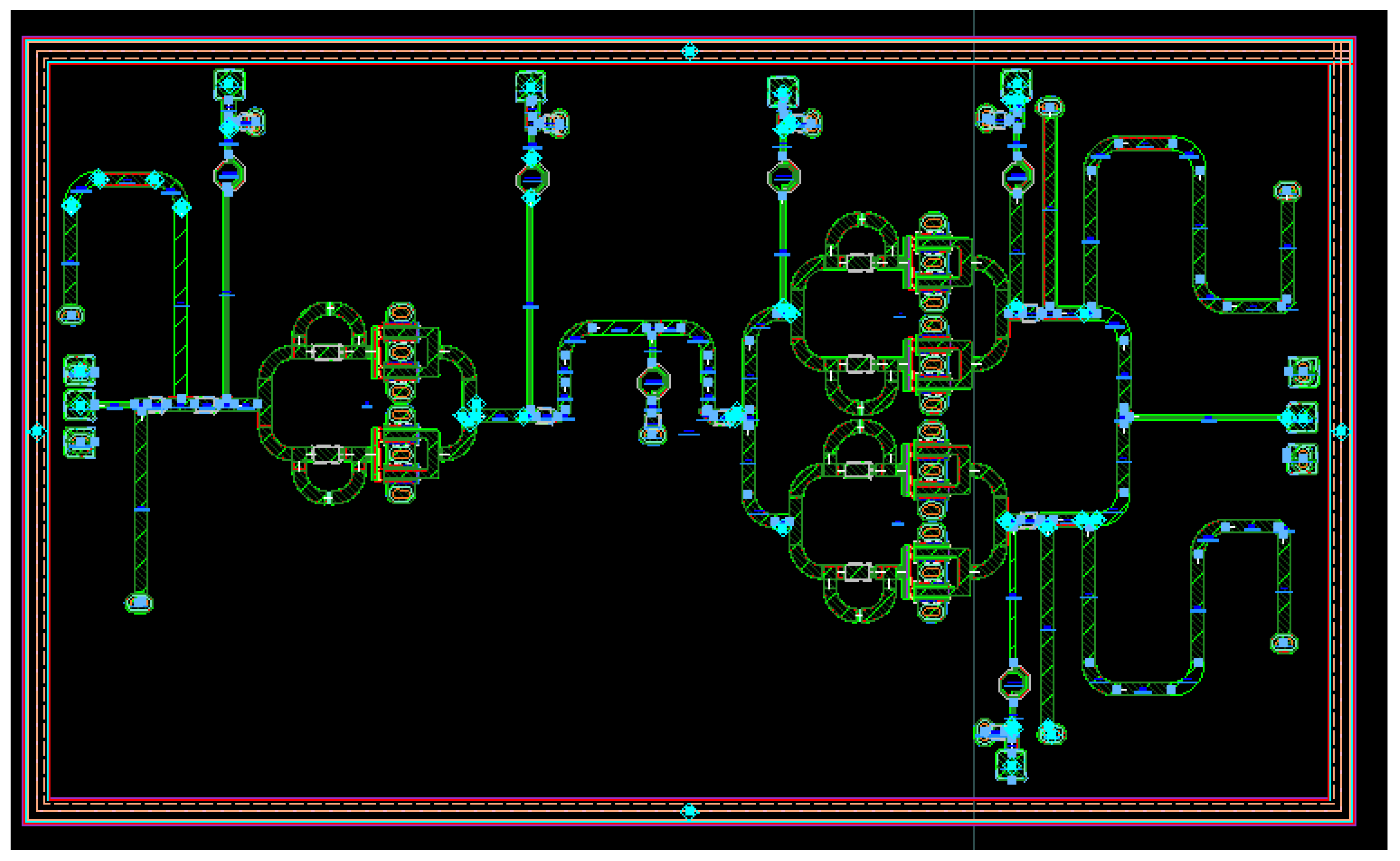
MMIC Layout Design Methodology For Microwave Circuits
 studylib.net
studylib.net
MMIC Layout Design Methodology for Microwave Circuits
Layout Design Of Elliptic Multilayer CPW MMIC LPF | Download Scientific
 www.researchgate.net
Layout Design of elliptic multilayer CPW MMIC LPF | Download Scientific ...
Phased Array GaN MMIC Reference Design
 www.eenewseurope.com
Phased array GaN MMIC reference design ...
Yap How-Siang On LinkedIn: MMIC Layout EM-Circuit Co-simulation Design
 www.linkedin.com
Yap How-Siang on LinkedIn: MMIC Layout EM-Circuit Co-simulation Design ...
MMIC Four Bit Phase Shifter Preliminary Design
 www.microwaves101.com
MMIC four bit phase shifter preliminary design
Mmic Power Amplifier Design Tutorial At Eve Collie Blog
 storage.googleapis.com
Mmic Power Amplifier Design Tutorial at Eve Collie blog
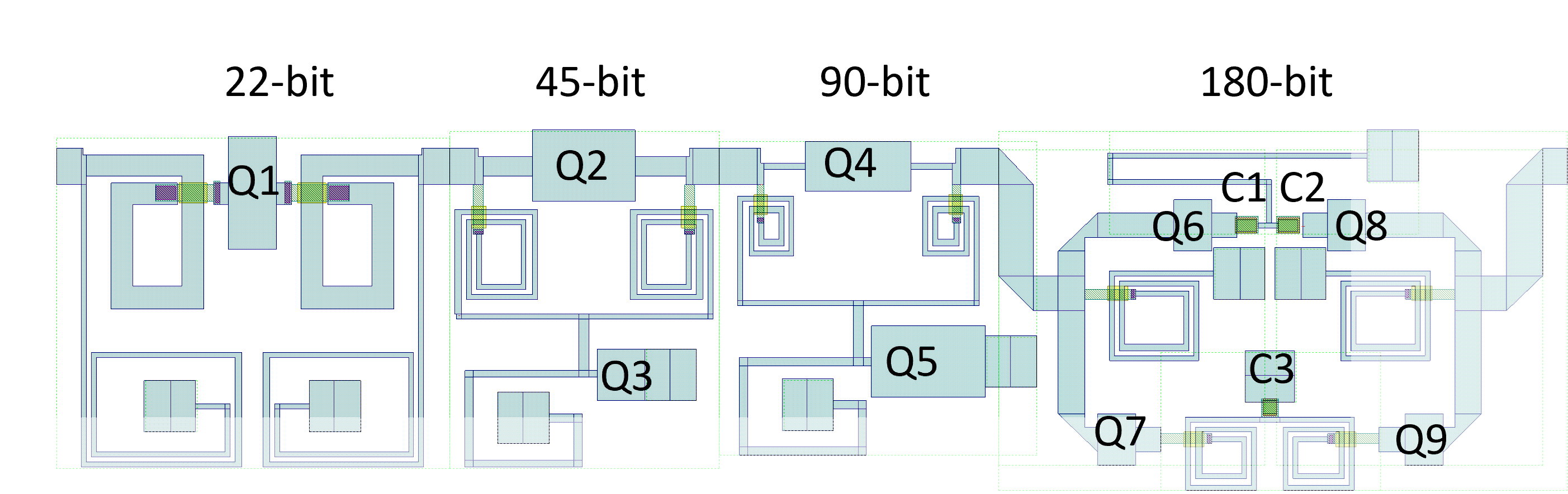
MMIC Phase Shifter 22 Degree Bit Design
 www.microwaves101.com
MMIC phase shifter 22 degree bit design
Accelerating MMIC, RF Module Design With ADS 2009 Update 1 | Microwave
 www.microwavejournal.com
Accelerating MMIC, RF Module Design with ADS 2009 Update 1 | Microwave ...
MMIC And RFIC
 www.prfi.com
MMIC and RFIC
Antenna Design And Rf Layout Guidelines - Design Talk
 design.udlvirtual.edu.pe
Antenna Design And Rf Layout Guidelines - Design Talk
Buy Base Universal RF Boards Ads And Download
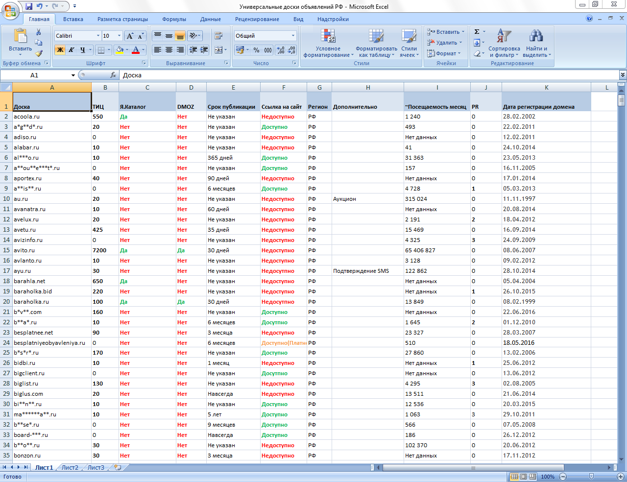 plati.ru
Buy Base universal RF boards ads and download
Antenna design and rf layout guidelines. 3 enhanced basics of rf/microwave pcb design. Phased array gan mmic reference design ...